BIG Solar-Wafer
Solar wafers enabled by lasers with high-performance deflection units
The current trend is toward large solar wafers enabled by lasers with high-performance deflection units
The deadline has been set! Just recently, the EU announced that it would be calling time on the sale of new cars with combustion engines by 2035. The ambitious goal of achieving carbon neutrality by 2050 had already been adopted, together with the intermediate target of slashing 55 percent of greenhouse gas emissions by 2030. And, although this new deadline did not take the automotive industry by surprise, it nonetheless appears to be a mammoth task with far-reaching consequences for everyone.
One of these is the reality that, unsurprisingly, more energy needs to be generated – in particular, green energy from renewable sources. And this now needs to be done at an even faster pace. Both fuel cell technology and the solar industry – once regarded as flagship technologies “made in Germany”– have gained huge momentum since Germany‘s decision to phase out nuclear energy. Since then, we have been witnessing a return to focussing on our own innovative capabilities. After all, Europe once led the way in solar energy development. However, due to the (politically motivated) reduction in subsidies, Europe couldn’t continue to compete with China, in particular due to costs. As a result, the European market collapsed and migrated to Asia. In 2020, fuelled by the effects of the coronavirus pandemic, Europe was forced to make the painful acknowledgement that too much global dependency has its drawbacks.“ Since then, however, Germany has been making strides in reducing our production and purchasing costs. In addition, transport costs in the EU are not as high, which is increasingly producing a competitive advantage for European manufacturers”. This is according to RAYLASE CEO Dr. Philipp Schön, who is also happy to report that “ our RAYLASE deflection units are making an important contribution to ensuring more efficient and cost-effective manufacturing of solar wafers in industrial production”.
Strong growth in the demand for solar wafers to meet increased energy requirements
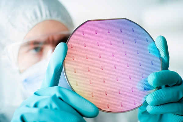
Round, square and rectangular solar wafers are the basis for photovoltaic energy production. They are used to create solar cells in which, by means of the photovoltaic effect, light is converted into energy. Global efforts are required to ensure the electrification of our future with green energy. After all, the hunger for energy in large economies like China and India is growing all the time with no end in sight. In fact, it is more likely to increase even further, according to Dr. Clark Lee, Key Account Manager at RAYLASE, who has intimate knowledge of the Asian market: “The global demand for ever-more efficient photovoltaic solutions has been increasing on a massive scale for years and will continue to do so in future”.
These markets today are already using a large number of solar wafers manufactured using the innovative PERC method (passivated emitter rear contact). The advantage of this method is that it is 20 % to 25 % more efficient than conventional methods at converting sunlight into energy when used in industrial mass production. The International Technology Roadmap for Photovoltaics (ITRPV) therefore assumes that PERC solar cells will have a global market share of more than 70 % by the year 2026. Recent years have also seen a growing trend toward larger solar wafers and modules, because they are proportionally more powerful.
In the updated 12th edition of the TRPV Roadmap for Photovoltaic 2021, which includes contributions from 56 international experts across the entire PV value chain, the German Mechanical Engineering Industry Association (VDMA) documents the current trend toward the consolidation and standardisation of three wafer sizes. According to the roadmap, in addition to 166-millimetre wafers, 210-millimetre wafers in particular will be considered in mass production in the future, as well as wafers with 182 millimetres. Smaller formats will gradually disappear from the market as a result. At present, the learning curve for photovoltaics is moving swiftly and steeply upwards in terms of chemical and metallic processes used in high-efficiency modules and larger solar wafer formats. The ITRPV report mentions a cumulative price reduction of
23.8 %. “Based on recent results, the trend is expected to continue along this experience curve over the next several years. This will be realized through a combination of several measures: improved and larger silicon wafers, implementation of cell perfections, optimized cell fronts and backs, refined layouts, the introduction of bifacial cell concepts, and optimized cell and module technologies.”
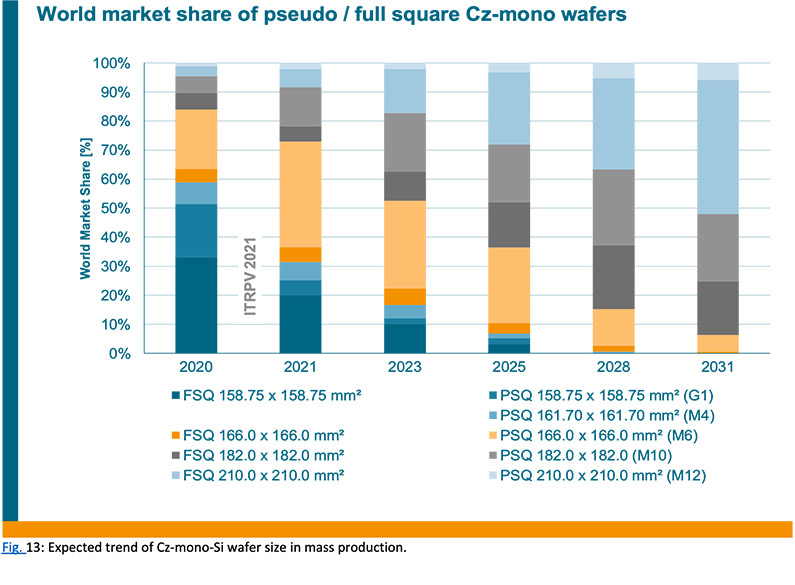
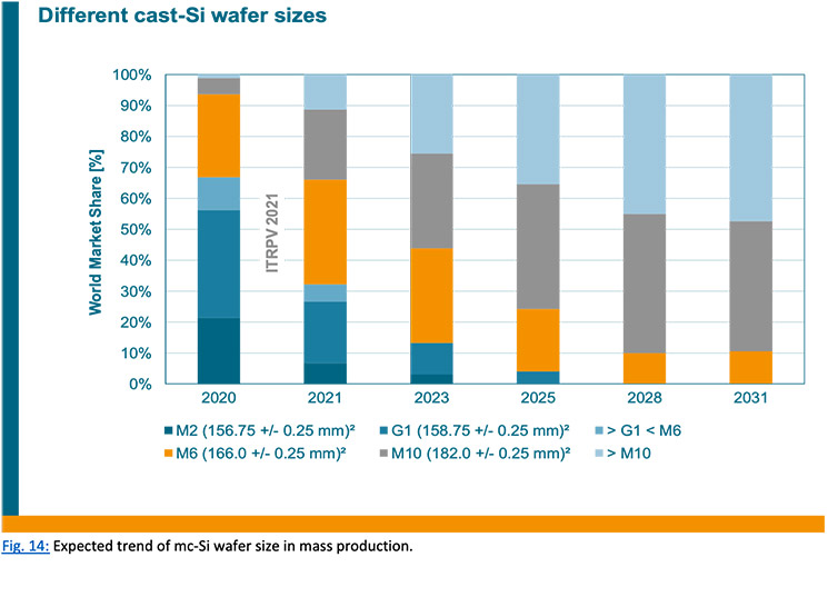
The chart from the ITRPV Roadmap 2021 clearly shows that wafer sizes such as M10 and M12 will dominate the markets in future. Quelle: ITRPV Roadmap 2021
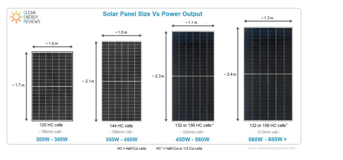
Large cells increase the power output of the entire PV module.
Source: Clean Energy Review
The importance of lasers in solar wafer production
Two proven methods improve the efficiency of the PERC PV cells mentioned above. These are laser contact opening (LCO) and laser doping in the selective emitter process, as described in the RAYLASE White Paper on next-generation solar wafer products.
As highlighted in the ITRPV Roadmap, the solar industry is currently moving away from the standard square solar cell with a size of 156 mm to larger wafers like the M10 (182 mm) or M12 (210 mm) to further reduce the manufacturing costs of wafers and increase their efficiency. The reason for this is that larger cells with a larger surface area, combined with larger wafers, create extremely powerful solar modules with a maximum output of up to 680 Watts. This alone increases panel efficiency by more than 22 %.

Renewable energies and their uses

Dr. Clark (H. S.) Lee, Sales Director Asien
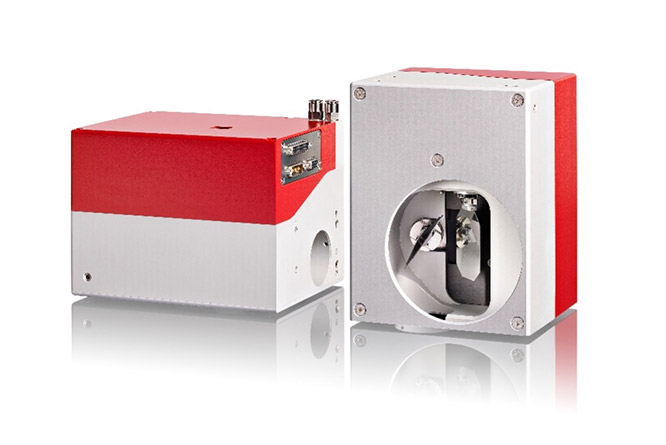
A good connection:Laser + SUPERSCAN IV-20 SOLAR
“Due to the strong demand for larger PV cell formats, we developed a 20 mm high-speed scanner as a prototype for large-format solar wafer production,” explains Clark Lee, who goes on to say that this innovation is “ unbeatable in terms of speed, precision and efficiency, and is one of a kind in today’s market”.
The SUPERSCAN IV-20 SOLAR from RAYLASE in the high-speed version with a larger aperture is connected to intelligent software for LCO wafer structuring – this is one of the company’s most innovative solutions for the solar industry.
THERE ARE VARIOUS CHALLENGES ASSOCIATED WITH WAFER PRODUCTION WITH DEFLECTION UNITS. THESE ARE SUMMARIZED IN THE STEPS BELOW:
- The industry needs larger PV cells
- These require larger wafer formats with larger modules
- This necessitates a larger field size for processing
- Which calls for a longer focal length in the optical elements
- This, in turn, enlarges the focal spot
- Which is, however, reduced in size by the larger aperture/ mirror to preserve the power density
“The challenge for our engineers was to maintain maximum speed while increasing the size of the mirrors and mechanics – so, in a sense, taking on more “baggage” –, without impacting the precision of the process as a result”, explains Clark Lee. This meant that RAYLASE faced the task of overcoming the restrictions of physics and providing solar panel manufacturers with software and controls to enable them to easily change the marking patterns on the wafers, such as solid, dashed or dotted lines.”
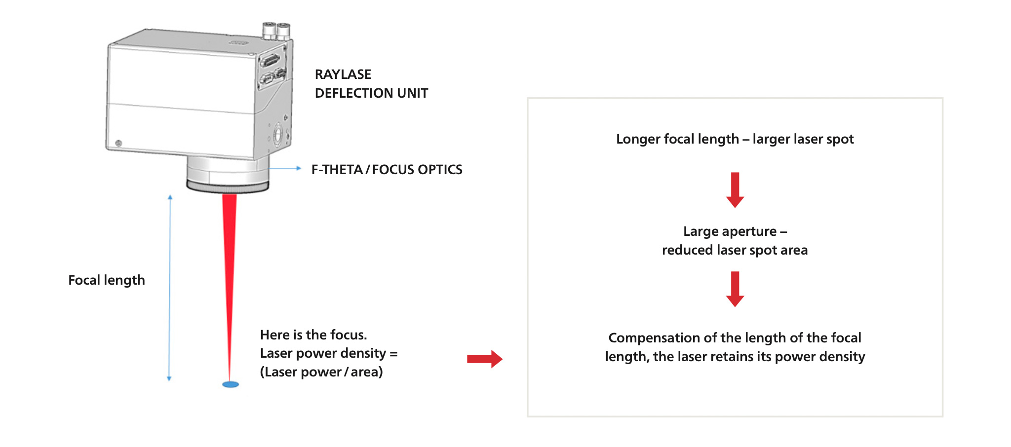
Solutions: Increasing throughput to 4,000 wafers per hour
In combination with an F-Theta lens with a long focal length, it is possible to achieve large field sizes without affecting the laser’s power density. The laser system also offers maximum speed, high-precision performance and extreme flexibility.
Product Manager Wolfgang Lehmann uses a detail to show how the dynamics are maintained: „To mark the wafer quickly and accurately, activating „SkyWriting“ does not slow down our deflection unit at the marking boundaries of the wafer, but simply switches off the laser. Outside the process field, the system‘s mirrors can be aligned to the 180° direction at almost full speed. We can merge the line segments into a single line‚ so that no deceleration or acceleration occurs at the “windows”. In this case, we use the “dashedline” feature so that the laser is only modulated in the relevant places.”

Wolfang Lehmann, Head of Product Management
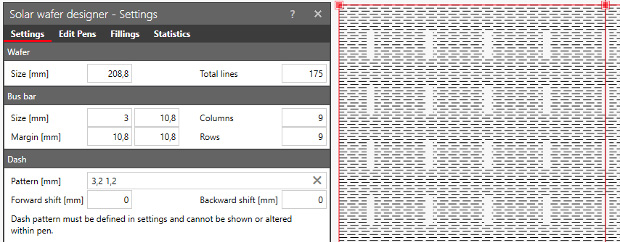
RAYGUIDE software from RAYLASE allows customer-specific design patterns for wafers to be imported or created.
Source: RAYLASE
SUPERSCAN IV-20 SOLAR
The SUPERSCAN IV-20 SOLAR 2-axis deflection unit is designed to meet the most rigorous performance requirements for high-speed, high-precision laser processing of solar cells. The digital control of the SUPERSCAN IV-20 SOLAR offers maximum speeds of up to 160 rad/s final speed. This corresponds to a speed of up to 52 m/s in the process field of an M12 wafer of 210 x 210 mm2. And, with the SP-ICE-3 control card and the corresponding RAYGUIDE software from RAYLASE, you are perfectly equipped to control the deflection units via SL2-100 protocol (20 BIT) or XY2-100 protocol (16 BIT).
Of course, machine manufacturers and integrators can also choose from a wide range of customization options. Lenses, protective glass, and mirror substrates and coatings are available for all standard laser types, wavelengths, light densities, focal lengths and processing areas.
Simply brilliant: the “solar wafer” plug-in
Of particular benefit to wafer manufacturers is the special solar wafer plug-in for our RAYGUIDE software, which significantly reduces processing time and ensures greater precision at maximum marking speed. To structure solar wafers, laser processing requires a pattern consisting of dashed lines. This pattern is broken up by rectangular spaces known as bus bars, which are evenly distributed over the wafer. Patterns are often defined using a DXF file and written to the laser processing software, which results in thousands of individual lines in a conventional import.
The solar wafer plug-in for the new software from RAYLASE combines these individual dashed lines into a greatly simplified dashed-line pattern, and the gaps in the pattern are generated precisely through laser power modulation. The new solution thus enables a faster and more direct adjustment of patterns. The Designer also enables a thoroughly streamlined workflow that bypasses the need to use DXF files. Ad-hoc changes to the wafer layout can also be made at any time. This is demonstrated in the “RAYGUIDE Solar Wafer Plug In” video.
Whether you already have experience in the solar area as a machine manufacturer and integrator or would like your company to enter this promising market, “we at RAYLASE are your ideal partner for design, integration, hardware, software and services relating to solar wafer manufacturing”, says Robert Kachel, Product Manager for software and control cards, highlighting the company’s innovative range of laser material processing solutions for solar wafers.
In this way, RAYLASE is making a meaningful contribution to creating a future society in which our climate and our environment are protected.
