Laser processes are an important part of the production of modern solar cells. In PERC solar cells, for example, the laser enables backside contacting of the cell by laser contact opening or selective laser doping of the semiconductor. In all these applications, it is usually necessary to laser very fine structures of a few micrometers with high precision. At the same time, productivity remains a key issue, because PV production only runs economically at the highest quantities. As a result, the cycle rate demanded by the solar industry is is over 3,600 wafers per hour.
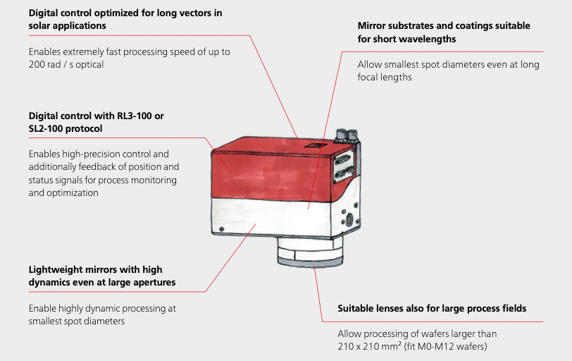
To reliably accomplish this task, it requires specialized high-speed scanners such as our SUPERSCAN IV-SOLAR series. With an accuracy of ± 10 μm, a marking speed of more than 60 m/s and highest dynamics due to the SiC mirrors, the 100 and 300 laser-written lines per wafer can be generated in less than 1 s and thus the SUPERSCAN IV-SOLAR ensures high production throughput and thus lower production costs.
With the SUPERSCAN IV 20 SOLAR, it is also possible to implement the necessary spot and speed requirements in larger process fields up to 210 x 210 mm2. This is an important aspect for the production of M12 solar wafers with larger dimensions.
Highest marking speed
Large processing fields

Smallest spot diameter
WHAT IS SPECIAL ABOUT THE SUPERSCAN IV SOLAR?
FAST AND PRECISE LASER PROCESSING OF SOLAR CELLS
The SUPERSCAN IV SOLAR is specially designed to meet the requirements of wafer processing in photovoltaics. It is important to select the optimum configuration for the deflection unit consisting of aperture, mirror substrates, coating and control electronics. Only this way the high requirements for speed, accuracy and dynamics can be achieved.
And it is precisely this combination that makes the SUPERSCAN IV-SOLAR series the optimal solution for your photovoltaic production. See for yourself:

FACTS & USE CASES
LASER CONTACT OPENING IN SOLAR CELL PRODUCTION
Solar wafer technology has been developing steadily for years. And especially in agile photovoltaic markets such as China, solar wafers produced with innovative processes like PERC ("Passivated Emitter Rear Contact") are used in large quantities. This is because the conversion efficiency of such wafers is in some cases more than 20 % higher than that of conventional BSF or HIT solar cells.
In the case of PERC solar cells, the higher energy conversion efficiency is enabled by a dielectric passivation layer (mostly Al2O3, SiO2, SiNx). Small contact openings are then created in this layer via laser ablation. This is done during Laser Contact Opening (LCO) by selectively removing the passi- vation layers via a dashed dot or line pattern.

Schematic drawing of a PERC solar cell and the Laser Contact Opening (LCO) process step. Source: T. Dullweber et al., Photovoltaics Internatio- nal, vol. 13 (2011), p. 77
High requirements on accuracy and throughput
In order to achieve optimum solar cell efficiency, the contact apertures must measure only a few 1/100 mm. This ensures that they do not unnecessarily expose silicon, which could lead to increased electron recombination. The placement of the contacts must be very precise to ensure correct alignment with the front contacts on the one hand and to avoid damaging the structure of the cell on the other. Repeatability of a few micrometers is required here. At the same time, the process step including handling time must not take longer than 1 second per wafer in order to optimally fit into the production process, which is typicslly designed for at least 3600 wafers per hour.
Specialized scanning solutions enable efficient production
For existing M0-M6 wafers, the SUPERSCAN IV 15 is an established solution. In combination with a 532 nm laser and an f = 255 mm f-theta objective, it achieves spot sizes smaller than 20μm and accuracies < ± 10 μm. Thanks to a tuning optimized for long vectors, the SUPERSCAN IV-15 reaches speeds of up to 200 rad/s or over 50 m/s in the field. This makes it possible to mark 100-300 lines per wafer in less than 500 ms and thus meet the requirements of the photovoltaic industry.
Larger wafers M12 wafers require new scanning solutions
However, the increasing size of solar wafers poses challenges for laser production. This is because existing scan systems cannot achieve the necessary processing fields of at least 210 x 201 mm2 without increasing the spot size. And scan systems with larger apertures typically do not offer the necessary dynamics and high speed.

The manufacturers of photovoltaic modules are relying on ever larger wafers. This allows solar modules to be produced more cost-effectively.
To support manufacturers in their shift towards larger wafers and thus cheaper solar modules, the SUPERSCAN IV 20 SOLAR was developed. With its lightweight SiC mirrors, optimized electronics and its special tuning, the SUPERSCAN IV 20 SOLAR offers speeds of 200 rad/s, just like the smaller deflection units. Additionally, the mirrors are optimized for use at a wavelength of 343nm, enabling even finer structures.
At the same time, a combination of the SUPERSCAN IV 20 SOLAR with a suitable f = 330 mm F-Theta lens provides the necessary larger processing fields for the production of M12 wafers and still allows a cycle rate of at least 1 wafer / second.
This allows the solar industry to further reduce production costs and ensures that the high demand for low-cost PV modules can be further met.
OPTIMAL ADD-ONS
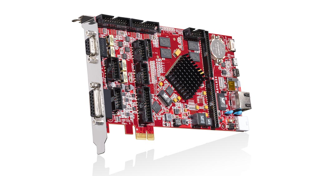
SP-ICE 3 CONTROL CARD: HIGHEST SPEED THANKS TO INTELLIGENT CONTROL

The high scan speeds in wafer production pose challenges for scan systems. Because, only if the velocity is kept constant, the individual pulses can be cleanly positioned on the wafer.
For this reason, the mirrors are only accelerated outside the processing area. A "skywriting" provides a very fast direction change of the beam outside the processing area without active laser power. Since these turn-around times can become quite relevant with up to 300 lines, it is important here to use a deflection unit with lightweight mirrors and low tracking distortion.
In addition, process time can be saved via intelligent software functions. At the windows of the “passivation layer”, line segments can be combined into a line using the "dashed line" feature of the SP-ICE-3. As a result, the laser is only modulated at the corresponding points and there is no deceleration or acceleration at all. This prevents valuable time from being wasted and increases the productivity of the process.
RAYGUIDE SOFTWARE: QUICK AND EASY OPTIMIZATION OF THE SCANNING PATTERN
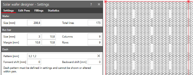
A special plus for wafer manufacturers is the RAYGUIDE software with its special solar wafer plug-in. Typically, a solar wafer laser process requires a pattern consisting of dash lines for structuring. It is interrupted by rectangular areas – “bus bars”, which are evenly distributed over the wafer. Often these patterns are created using a DXF file and loaded into the laser process software, which results in thousands of individual dashes when imported conventionally

RAYLASE software RAYGUIDE can import or design the customer's own design pattern for wafers.
The RAYGUIDE solar wafer plug-in combines individual dash lines into a dash line pattern. This way, the gaps in the pattern are precisely created by modulating the laser power instead of marking individual vectors. In addition, the software also allows faster and more direct adaptation of the patterns. As a result, ad hoc changes to the wafer layout can be made easily and conveniently with it. Furthermore, the “Designer” offers a fundamental streamlining of the workflow, since the detour via DXF files is eliminated.
OTHER SUITABLE ACCESSORIES
CAMERA ADAPTER
FOR ON-AXIS PROCESS MONITORING
With our camera adapter and the Machine Vision Con- trol components, the deflection unit can be expanded to include process monitoring.
LENSES & MORE
SUITABLE OPTICS FOR EVERY APPLICATION
F-theta lenses, protective glasses, mirror substrates and coatings are available for all common laser types, wavelengths, power densities, focal lengths and pro- cessing fields.
GOOD REASONS TO CHOOSE RAYLASE
THIS MAKES RAYLASE SPECIAL
Technical specifications are important and often decisive. But at RAYLASE, we believe that there is more to it than pure technology that matters. For this reason, we are your partner for reliable and successful laser processes and offer more than just technical components.
Systems view instead of components
Modern production systems for laser processing are usually designed specifically for one process step and are highly optimized. It is therefore important to consider the interplay with the other machine components when selecting suitable beam deflection units. At RAYLASE, we therefore always have the entire solution in mind and offer our customers assistance in putting together suitable components.
Broad application knowledge
For many processes, the beam deflection unit is a decisive component. Often it determines whether the desired spot parameters and processing speeds can be implemented on the component. To identify the optimal solution here, we support our customers in selecting the right beam delivery components and sensor technology. and perform simulations of the laser processes developed by our customers. In addition, we provide support in the parameterization of the laser and deflection unit or software functionality through the experts at our Technical Competence Center TCC.
On-site support for implementation and service
Our customers are the experts for their application - we are the experts for our beam deflection units.That's why we support our customers during the commissioning of our products - if necessary also directly on site. In this way, we at RAYLASE ensure that our system is optimally adjusted and permanently delivers what it is capable of.
Education & training on the system
Modern laser deflection units are complex systems. Therefore, it is important to have a good knowledge of their characteristics. Because only when users know how the various parameters interact the optimum process becomes possible. For this reason, we at RAYLASE put a high priority on training for our products. In addition, we also offer our customers on-site training directly on the system, if required, to enable users to operate the system independently.
The POWER OF WE
Together you achieve more. At RAYLASE, we are convinced about this. That's why we place great value on cooperation in a spirit of partnership and open communication at equal level – from expert to expert. Because only when we jointly find the best solution and successful integrate it into the machine, everyone involved benefits in the end - our customers, us and also the end users.
FEATURES
- Digital control optimized for long vectors in solar applications
- Digital control with RL3-100 or SL2-100 protocol
- Lightweight mirrors with high dynamics even at large apertures
- Mirror substrates and coatings suitable for short wavelengths
- Suitable lenses also for large process fields
